OUR RESEARCH ARCHIVE
Below we list a number of older research topics that we have worked on:
Cambridge Graphene Centre
The Antennas Group (with involvement led by Prof. Yang Hao) is an active member of a consortium led by University of Cambridge that has proposed a programme of innovative and adventurous research, with an emphasis on applications, uniquely placed to translate this vision into reality. The research consortium, led by engineers, brings together a diverse team with world-leading expertise in graphene, carbon electronics, antennas, wearable communications, batteries and supercapacitors. The consortium has strong alignment with industry needs and engage as project partners potential users.
The programme consists of related activities built around the central challenge of flexible and energy efficient (opto)electronics, for which graphene is a unique enabling platform. This will be achieved through four main themes:
- T1: growth, transfer and printing;
- T2: energy;
- T3: connectivity (led by QMUL);
- T4: detectors.
The vision is to take graphene from a state of raw potential to a point where it can revolutionise flexible, wearable and transparent (opto)electronics, with a manifold return for UK, in innovation and exploitation. Graphene has benefits both in terms of cost-advantage, and uniqueness of attributes and performance. It will enable cheap, energy autonomous and disposable devices and communication systems, integrated in transparent and flexible surfaces, with application to smart homes, industrial processes, environmental monitoring, personal healthcare and more. This will lead to ultimate device wearability, new user interfaces and novel interaction paradigms, with new opportunities in communication, gaming, media, social networking, sport and wellness. By enabling flexible (opto)electronics, graphene will allow the exploitation of the existing knowledge base and infrastructure of companies working on organic electronics (organic LEDs, conductive polymers, printable electronics), and a unique synergistic framework for collecting and underpinning many distributed technical competences.
Photonic Antennas with Integrated Optical Transducers
Distribution of multiple wireless services including GSM/UMTS, TETRA and WLAN via installed fibres in buildings has become a commercial reality because of the broadband, low-loss and modulation format agnostic features that the radio-over-fibre technique offers. Distributing multiple services in a radio over fibre system also centralise the management of telecom and network equipment. Photonic antennas find applications in such in-building scenarios by acting as the interface between the installed fibre infrastructure and the wireless service users. The cost of manufacturing such photonic antennas can potentially be reduced further if they are integrated directly with the optoelectronic components performing the optical-electrical and electrical-optical conversions, and this has been the motivation and the subject of the project.
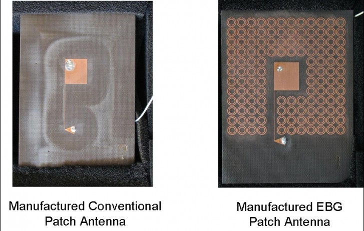
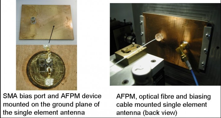
Photonic Antennas has been a collaborative project between University College London (UCL), Queen Mary University of London (QMUL) and Rutherford Appleton Laboratory (RAL). UCL has been responsible for the design, development and fabrication of the Asymmetric Fabry-Perot Modulator/detector (AFPM) which is used as the key optical transducers functioning simultaneously as an optical intensity modulator and a photodetector. QMUL has been responsible for designing and fabricating a ring of Electromagnetic Bandgap (EBG) and non-EBG patch antennas. RAL has been responsible for developing a technology to package the AFPM from UCL with a connectorised optical fibre pigtail which is critical if the device is to be deployed outside the laboratory environment. RAL has also been responsible for integration of the AFPMs with the antennas from QMUL resulting in the ultimate photonic antennas.
Flat Lens Modelling and Layered LHM Structures
Left-handed materials (LHMs) are those engineering composites that the electric permittivity and the magnetic permeability of a material are both negative. This was noted theoretically some time ago: in 1968, Victor Veselago of the Lebedev Physics Institute in Moscow described LHMs exhibiting an anti-parallel nature in its wave and Poynting vectors. This is opposite to conventional materials, within which electromagnetic waves carry energy in the same direction as they propagate, following what's called a right-hand rule. Exciting possible electrodynamic properties, such as a reverse Doppler shift, Cherenkov radiation and an inverse Snell effect, were identified. However, because of the unavailability of LHMs at that time, his idea was forgotten until recently, when Prof. Pendry (UK) demonstrated that materials with an array of split ring resonators (SRRs) produce negative permeability over certain frequency bands. Soon afterwards, by combining a two-dimensional (2D) array of SRRs interspersed with a 2D array of wires, Prof. Smith’s Group (USA) demonstrated, for the first time, the existence of LHMs.
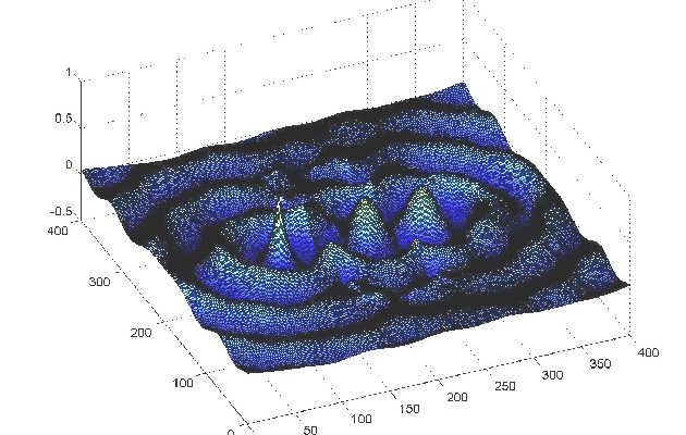
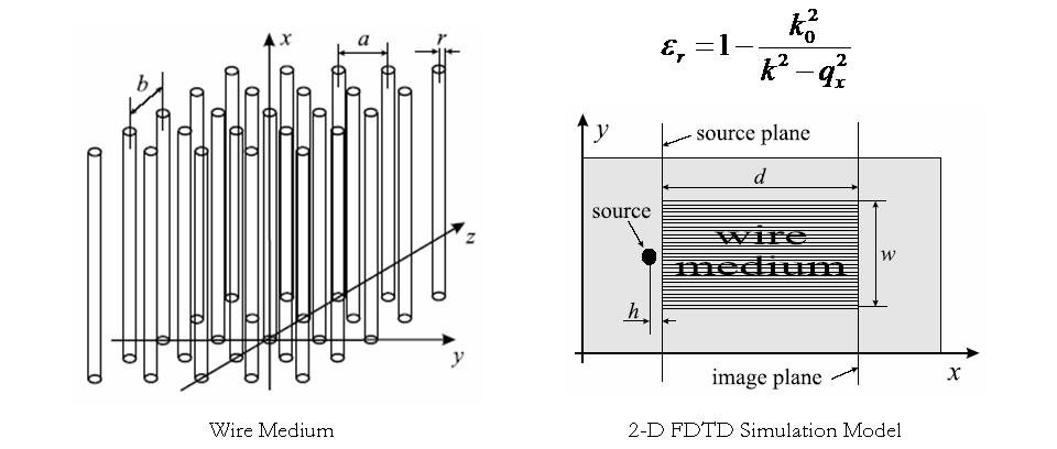
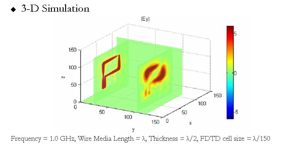
Wire Medium Imaging
We have investigated, through numerical simulation, whether or not the finite transverse dimensions of LHM slabs influence the quality of their sub-wavelength imaging. However, in practice, the fabrication of left-handed media remains problematic, since it requires the creation of negative permeability, which does not exist in nature. Furthermore, currently available designs of the left-handed media are very lossy at both microwave and optical frequencies, which restricts and even prevents their use in sub-wavelength imaging applications.
There is an alternative approach to sub-wavelength imaging, in the sense of mapping the source distribution in one plane onto another (the imaging plane). This approach involves neither the use of left-handed media nor does it capitalize on negative refraction or amplification of evanescent waves, which has been referred to as canalization. It is based on transporting both the propagating and evanescent spectra of a source by transforming them into propagating waves inside a slab of specially designed materials. Then, these propagating modes are capable of transporting sub-wavelength images from one interface of the slab to the other. The source must be placed very close to the front interface of the slab in order to minimize the degradation of its spectrum, which occurs when the fields propagate in free space. It is also necessary to minimize the reflection from the slab via an appropriate choice of its thickness. This is done by tuning the slab thickness for Fabry-Perot resonance, to reduce reflections from its interface for a wide range of angles of incidence, and minimize the interfering interactions between the source and the slab that can distort the image.
The material operating in the canalisation regime should have a flat iso-frequency contour, implying that it should support waves travelling in a certain direction with fixed phase velocity for any transverse wave vectors. The materials that fulfil this requirement are available at both microwave and optical frequency ranges. One such artificial material is the wire medium, comprised a regular array of parallel metallic wires.
95GHz Woodpile EBG Antennas
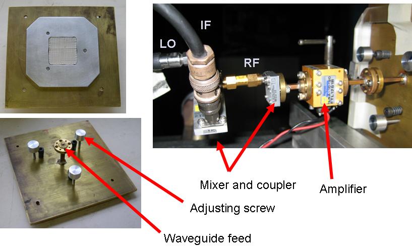
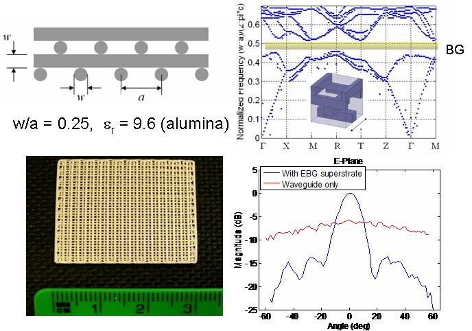
Millimetre wave systems are becoming increasingly important in many applications because they can provide wider bandwidth for transmitting large amount of data and better resolution in radar systems. Electromagnetic Bandgap (EBG) structures, a class of metamaterial also known as photonic bandgap structures (PBG) in optics, are now finding numerous applications at microwave and millimetre wave frequencies . The full potential of EBG structures can be utilised with a full three dimensional (3D) bandgap. Thus, rapid and cost-effective fabrication techniques for 3D EBG structures are of significant importance. A woodpile structure, shown in the figure, exhibits a full 3D bandgap and can be easily fabricated for applications at microwave frequencies using columns of individually machined dielectric rods . However, at millimetre wave frequencies, conventional machining would not be convenient because of small dimensions (50–500 mm). Various sophisticated techniques such as silicon lithography are available for microstructures, but those are more appropriate for terahertz and photonic wavelength applications, and would be costly to fabricate 3D structures with large number of layers for applications at W-band (75-110 GHz). In this work, we present a direct rapid prototyping method for constructing 3D EBG materials for millimetre-wave applications, with a possible extension to higher frequencies based on extrusion free-forming of ceramic materials. The proposed fabrication method can also be versatile for constructing curved geometries and creating defects in layered structures.
